Closed-Loop Control Circuit:
One of the most important methods to control system is ‘’ proportional-integral controllers,” which are commonly used in many projects and applications in the engineering industry. The reason for that is their simplicity in terms of use, and they provide enough compensation for errors. Additionally, PI controllers reduce the number of parameters in the system, and it is also able to remove forced oscillations. Furthermore, those controllers help a lot to eliminate the disturbances of signals. [18]
Voltage Controller:
In this project, only P&I controllers are going to be used since the differential gain is mostly needed in slower mechanical systems. The first use of PI controllers is the control of one parameter, in this case, the PI control circuit is the best choice controlling the output voltage of a converter. [19]
Below, is a block diagram that shows the general control circuitry.
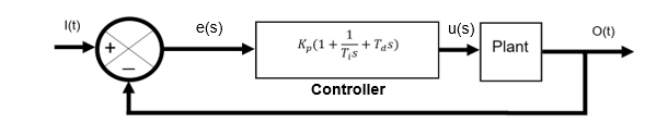
Figure 3‑9 general control circuitry block diagram.
From the block diagram above, the input to the controller is the error e(s), and the output is the input to the plant, which is the DC-DC converter u(s). The input for the plant is the waveform that controls the duty cycle of the switch.
The transfer function for the PI controller is:

High-Frequency Active PFC:
Now as required, the PF needs to be above 0.9, and for that, a proper Power Factor Correction (PFC) method is required. Passive PFC is one method for improving the power factor, passive PFC include passive elements such as inductors and capacitors. Passive PFC is not going to be used since it occupies a large space and slower in regulating the output when compared to active PFC [8]. High Frequency Active PFC is a method that uses switches as circuit elements instead of passive elements and works with a very high switching frequency, thus named high frequency active PFC. This method is more suitable for PFC since it does not occupy much space and responds swiftly [8].
Selection of P/I Coefficients:
The control unit chosen for PFC was the PI control unit. This unit is simply the heart of the control unit in which it provides the basic commands for the input and output readings based on the previous readings. The proportional unit is meant to influence the input readings by large, while the integrator is supposed to reduce the steady-state error.
Trail and Error:
Since the control of the output voltage for the buck contains one PI controller, and the system is second order. () and () that provides accurate results can be easily obtained with no time, () and () were selected to be 0.1 for both in this case. On the other hand, the rectifier boost circuitry proves to be more complicated. In this step, it has tried varying the values of the P/I coefficients for both the PI units. But, in this case, four unknowns have generated; thus, it is needed guidance for where to start. The two consecutive PI units control the input current quality and the output voltage response when varying the outer PI unit’s coefficients, a greater change on the input current THD appears. Now when the proportional coefficient KP was put very small, the THD of the input was reduced drastically, but reducing the furthermore makes the overshoot at the transient state very large. When it comes to the integrator coefficient , the THD was slightly decreased as the was decreased.
As a result of this method the Maximum overshoot of output voltage, and the settling time for the output voltage. The values chosen were = 0.05, and = 20. The inner PI unit variation is not very difficult as the change in both and Ki does not put much change on the input THD, the most important thing is that the ratio between / for the outer PI unit is larger than that for the inner PI unit. Otherwise, the THD for the input increases drastically. The values chosen were = 10, and = 100 for the inner PI controller. [11]
Results of the Closed Loop Buck converter
As stated above, = 0.1, and = 0.1 for controlling the output voltage of the buck converter. The circuit design and results are shown below.
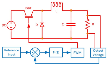
Figure 3‑10: Buck converter with closed-loop.
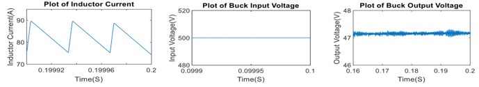
Figure 3‑11: Closed-loop Buck Results.
Results of the Closed Loop Rectifier-Boost converter
Now, the main reason the boost converter [10] is used in the design of the OBC is that the control circuit is connected between the rectifier and the boost converter. And by controlling the duty cycle of the switching frequency, both the input (THD and PF) are improved, and the output voltage is improved. The circuit of the design is shown below. [16]
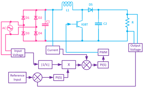
Figure 3‑12: Boost Converter Connected to PFC Circuit.
The circuit shown above illustrates the PFC control circuit connected between the rectifier and the boost converter. The circuit takes four inputs and provides one varying output. The input parameters are the AC input voltage, output voltage, reference voltage, and inductor current. While the output is the Pulse-Width Modulation (PWM) connected to the IGBT for controlling the duty cycle of the switching frequency going through the IGBT. The circuit also includes two PI control units, one PI (outer PI) for controlling the output voltage, and the inner PI unit for correcting the input current THD and PF. Note that the THD was measured to be 8.544%, and the power factor calculated to be 0.996. Below are plots of the output voltage and input current.
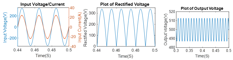
Figure 3‑13: Closed-Loop Boost.
Results of the Fully Cascaded Circuitry
Overall, all the systems discussed earlier were connected; the system consisted of a single-phase voltage source that is connected to OBC circuitry. The supply connected first to the full-bridge rectifier, which changes the AC voltage to DC. The output of the rectifier is then connected to a boost converter that is supposed to increase the voltage level to 500 V. After that; a buck converter was used to step down the voltage to 48 V where that is the voltage level of the load-batteries- that are connected to the output of the buck converter. When the two converters were cascaded, a slight change in the readings arises-as expected- but the control units still managed to minimize any unwanted variations in the desired parameters such as the output voltage and the input current THD and PF. [22]
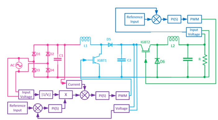
Figure 3‑14: Closed -Loop Full Circuit Simulation.
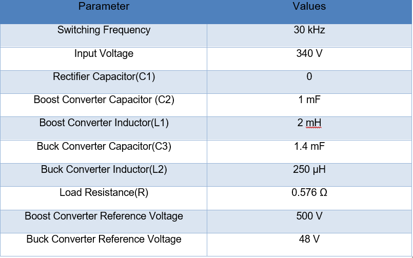
Now, when looking at the above circuit, it shows the rectifier followed by a boost after that a buck converter. There are two control circuits with three PI units that are responsible for voltage regulation and PFC. When it comes to the parameters used in this design, there were some changes for the system to function correctly. For instance, the capacitor after the rectifier was not needed anymore in the circuit; this was because there are parallel capacitors after the converters that do the filtering needed for obtaining a sharp DC voltage. In other words, this capacitor was removed. Additionally, all capacitors after the converters were given a high value (at least 1 mF) as assumed by the design of the converters. Furthermore, the value of the inductor in the boost converter was increased so that it provides additional filtering of the undesired harmonics in the input current. This made the THD falls to a low value, which allowed to adjust the values of the PI controller in the boost/rectifier control circuit so that the transient time is decreased for both the output voltage and input current of the total cascaded circuit [18]. Finally, the switching frequency for both the IGBT was 30 kHz, while the control circuits control the duty cycle for proper results. Below are plots of results after the construction of the full simulation circuit.
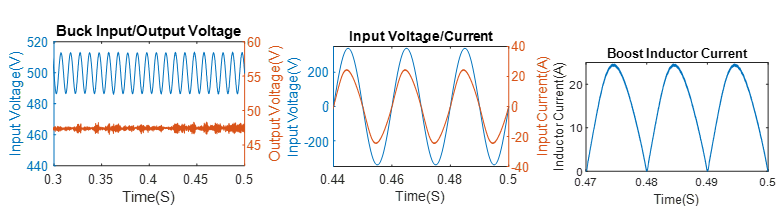
Figure 3‑15: Closed-Loop Cascaded (Full OBC) Results.
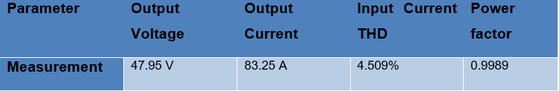
The value of the parameters used are presented in Table 3‑3 below:
Table 3‑3: OBC Parameters.
 And the results are shown in Table 3‑4 below:
Table 3‑4: OBC combined Parameters.