Full Wave Rectifier (FWR):
The FWR is a circuit that produces a dc voltage for an AC input voltage, or a voltage with high DC component. The FWR is followed by a capacitor to reduce the ripple in the output voltage. The equation for calculating the ripple of the output voltage is: [14]
![]()
The circuit is simulated below.
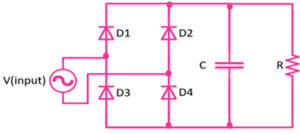
Figure 3‑1: Full Wave Rectifier.
The values placed initially are Vi = 340 V, C = 50 mF, and R = 0.576 Ω. And the average rectified voltage was 285.1 V. An increase in the capacitor helps to reduce the voltage ripples. But it is not needed to be increased rapidly other OBC components will include capacitors that provide better filtering of the voltage ripples. The result of the input voltage and the rectified voltage is shown below. [15]
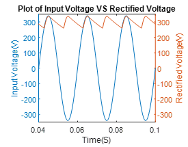
Figure 3‑2: Input Voltage Compared to Rectified Voltage.
DC-DC Boost Converter:
The boost converter is a switching converter that changes the dc voltage level from a low level to a high level. It operates by periodically switching on and off a switch, the switch used is the Insulated-Gate Bipolar Transistor (IGBT). However, the Boost converter operates in Continuous Conduction Mode (CCM), meaning that the inductor current is always above zero, and the value of the capacitor is high for proper filtering of the output voltage. The design is shown below. [16]
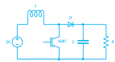
Figure 3‑3: Boost Converter.
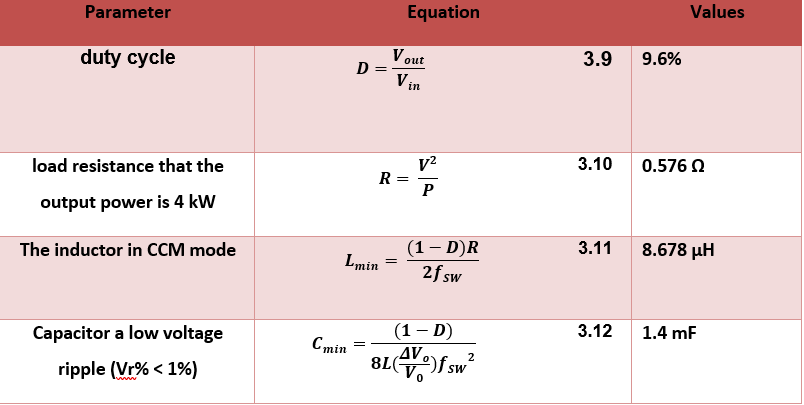
The boost converter takes a dc voltage equal to 340 V from the rectifier and boosts it to 500 V and the switching frequency equal to 30 kHz the calculation will be:
Table 3‑1: Boost converter parameters.
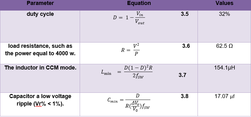
The value of the inductor chosen was L = 160 µH, and C = 20 µF. The results are shown below.
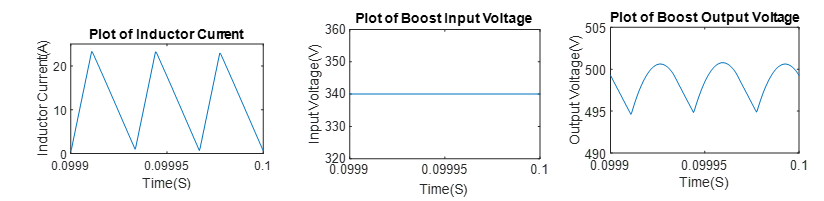
Figure 3‑4: Boost Converter.
DC-DC Buck Converter:
The buck converter is a switching converter that lowers the voltage level of a dc voltage source depending on the duty cycle of the switch. However, the components used as the boost converter, but the placement of the components is different. The converter is designed to operate in the CCM, and the capacitor is selected to be large. The design is shown below. [17]
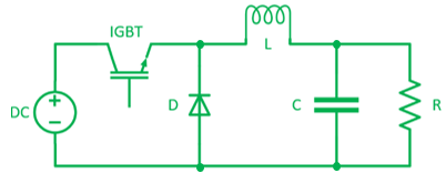
Figure 3‑5: DC-DC Buck Converter.
The input voltage to the buck converter is the output voltage of the boost converter, 500 V, while the output is minimized to 48 V with the same switching frequency 30 kHz, the parameters obtained as shown below. [17]
Table 3‑2: Buck parameters.
The value of the inductor chosen was L = 9 µH, and C = 1.4 mF. The results are shown below.
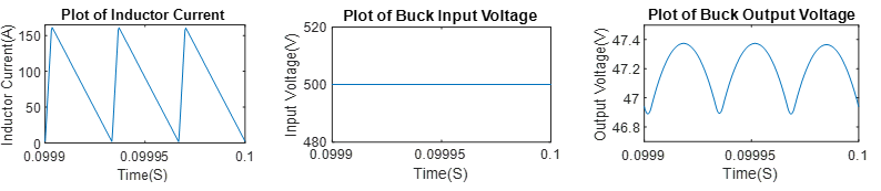
Figure 3‑6: Buck Converter.
Cascaded Open Loop Circuit:
In this part, all the circuits explained above, starting from the rectifier followed by the boost converter. Then the buck converter is going to be connected simultaneously without any changes in the component’s values specified above. For instance, the output of the rectifier is being filtered in both the boost and a buck converter, which makes it less significant to put a capacitor after the diode bridge. Additionally, the input to the boost converter is not an ideal DC voltage, which is going to result in variation in the readings for the results. Similarly, the buck converter is taking input voltage from the boost converter, which is not ideal dc voltage. Finally, the cascading of all three circuits makes the inductor and capacitor in one circuit affecting the readings in another circuit, while all power losses are added together. The circuit for the cascaded circuit is shown below. [19]
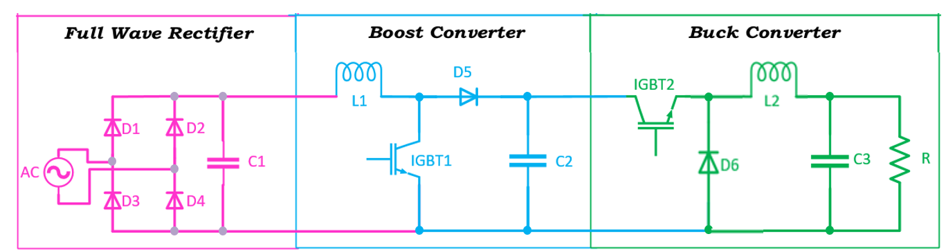
Figure 3‑7 Open Circuit OBC.
The results are shown below.
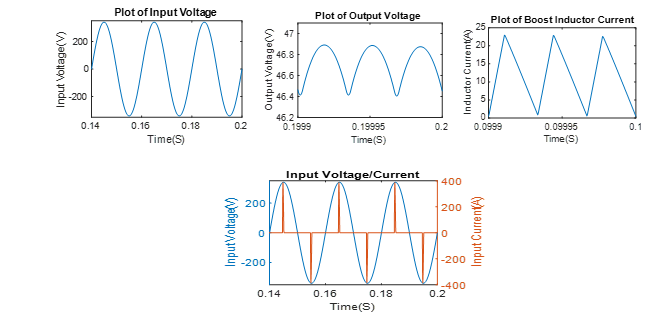
Figure 3‑8: Cascaded Open Loop Circuit.
From the above plots, the average output voltage was Vo = 46.45 V, while the output current Io= 80.64A.
Ideally, Vo needs to be 48 V, and Io needs to be 83.3 A. But since there is a power loss in the circuit components, including the switches, the power resulting from the open-loop OBC is 3745.7 W.
Both the inductors operate in the CCM as shown by their plots. Finally, the input current is very distorted because of the diode bridge and the converter circuits. The total harmonic distortion was calculated to be THD = 342.1%. The power factor was calculated to be 0.280. This means that the circuit needs additional adjustments to meet the input current requirement as well as adjusting the voltage level of the load voltage. A control circuit is presented for improving these parameters.