Selection and Characterization of the Foot Pressure Measuring Sensor
The criteria used for selecting the appropriate force measuring sensor to be used in a foot sole are as follows:
- The response of the sensor against a dynamic force
- Effective working range of the sensor (compared to average under feet vGRF of an adult)
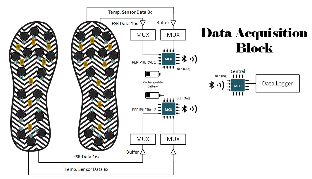
And the data acquisition block diagram is shown below:
Three common types of sensors were tested for this purpose viz.
- Force Sensitive Resistors (FSRs)
- Piezoelectric Sensors
- Velostat Sheet
The sensors were tested for their response of dynamic pressure since during locomotion, the person’s feet will apply dynamic pressure (variable over instant) on the sensors placed in the foot sole, and among the three types of sensor, FSRs were found to be the most suitable for placing on the insole. The characterization curves and other details of the sensor characterization process are out of the scope of this discussion.
Even though FSRs were selected as they were found to be the most suitable to be used in an insole after testing their dynamic response, using FSRs alone (by connecting FSRs in series from the power supply to the ground) will not provide any useful output since FSR is just a “variable resistor which is reactive to force applied on it.” FSR based applications (including this one) require reading the response of the FSR (change in resistance; that’s what makes them Force Sensitive Resistors) with respect to the force applied on it using the Analog to Digital Converter (ADC) of the microcontroller. For this purpose, a voltage divider circuit needs to be implemented for each FSR, as shown in the Figure below.
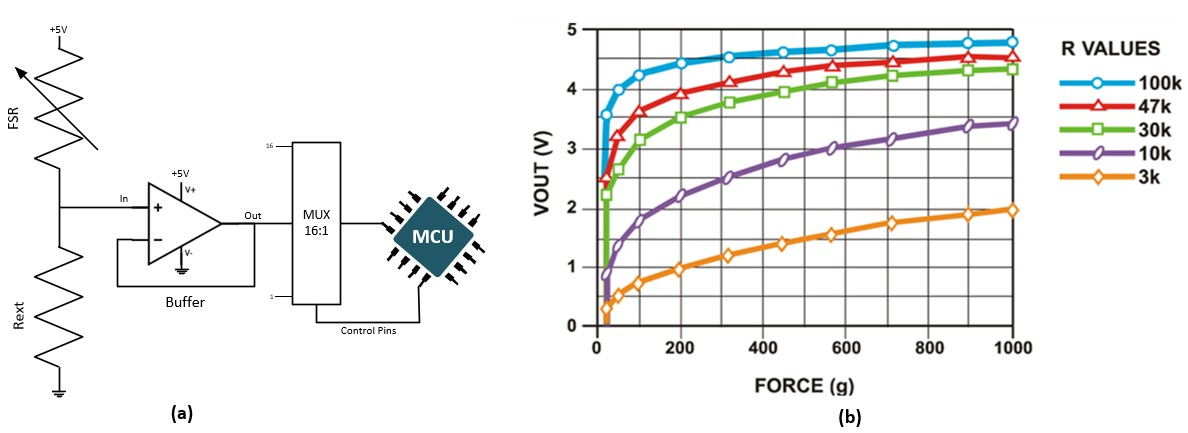
Figure 1 (a) refers to voltage divider circuit to take FSR measurements.
Figure 1 (b) refers to voltage output response for different values of Pull-Down (or Pull-Up) resistor with response to force applied on the FSR .
The equation for the voltage divider is as follows:
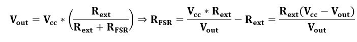
So, the voltage divider circuit will be used to measure the voltage across the external resistance, which in turn, will be used to measure the resistance of the FSR using the equation above through the micro controller acting as a peripheral.
Selection and Calibration of the Temperature Sensor
Temperature imbalance occurs under the feet of DFU patients and diabetic patients with a critical risk of being affected by DFU. Literature shows that between a normal foot and a foot with a risk of DFU, there is a minimum temperature difference of 2.2 . While monitoring this parameter, some regions of both feet should be observed, and any imbalance in temperature between corresponding regions (under feet) which goes beyond this threshold (2.2 ) and an imbalance in the person’s Gait Cycle (recorded by FSRs in the insole) should be forecasted as critical to be affected with DFU. Three types of commonly used temperature sensors have been considered for this purpose viz.
- Thermostats
- Resistance Temperature Detectors (RTDs)
- Thermistors
Among them, Thermistors were chosen due to some important reasons:
- The most important reason was that the Thermistors could be hooked up easily using the same voltage divider circuit as FSRs, as shown in Figure 1 (a). Since Thermistors work on Resistance change due to temperature (also RTDs, but their building material is different), voltage dividers work perfectly on them, just like FSRs. It made the circuit design for PCB lot easier and helped in keeping its size minimum. On the contrary, RTDs require a Wheatstone Bridge for each of the sensors. Placing eight bridges on the printed circuit board (PCB) would drastically increase its size. The thermostats are not suitable for this application due to their nature of work.
- The foot temperature of a person can vary from 15 (when the feet are cold during cold season) to about 37.5 during the summer (the study was done on normal people when they were awake).Diabetic patients with DFU or the potential of having it soon will have inflammation in the places of infection under feet. Since the aim is to find the hotness of the feet, the suitable working range of the temperature sensor was chosen as 20 to 50 . Selecting this range was crucial for the calibration of the sensor, which is discussed afterward. Now, Thermistors work very well within this range, and their response is close to linear. Adding to the factor mentioned in the previous point, this made Thermistors very much suitable for this task.
- Thermistors have very low response time, i.e., responses very fast, faster than RTDs and Thermocouples. Even though it is not a must for this application since temperature readings will just be used to find (corresponding) differences (i.e., no Machine Learning involved), having a fast response is not a critical need. But it is always a plus point to have so!
Selecting Thermistors as the temperature sensor was not enough since Thermistors (and any other sensor) comes into various packaging differed by size, shape, color, and advanced options like packaging material, water/thermal proofing, etc. For the insole design, the required properties of the temperature sensor module should be as follows:
- Flexibility: Firstly, the sensor will be embedded into the insole, which will be worn by a person under test. So, the sensor module must be flexible in order to ensure that the insole is not creating any impedance on the subject while walking (which might affect the gait cycle and provide biased data).
- Small Size: The sensing module should be small since temperature readings from various points under the feet need to be taken. Using sensors with the big surface area will not only block the FSRs but also will fail to provide the temperature data of a small section.
- Durability: The sensor module should be durable enough along with its flexibility since the insole will be worn inside a shoe. It needs to withstand shear, lateral, and vertical pressure applied to it while walking. So, the sensor module should have a certain degree of durability, not too fragile. It is also indirectly related to flexibility (in order to withstand shear pressures and bends).
- Temperature Response: The temperature response of the sensor module need not be very fast or dynamic like the FSRs since the temperature record need not be instantaneous. But having a fast response and a high sampling rate, if it does not overwhelm the hardware is always a plus point.
- Temperature Range: Temperature range should be able to contain the peak temperature readings from feet under any condition. The chosen module’s working range is between -30 C to 90 C, which contains the required measuring range (20 to 50 ) mentioned beforehand.
- Waterproofing: The sweating occurring (for some people it is more acute) in the leg after wearing the shoe for more than a few minutes is tackled by using waterproof temperature (also FSR) sensor modules.
The figure below shows a picture of the chosen Thermistor (10k NTC Thermistor Module from Littlefuse):
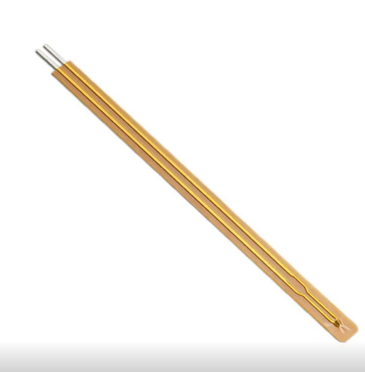
Based on these criteria, the temperature sensor module shown in the Figure above was chosen for the insole design. The sensor is an NTC (Negative Temperature Coefficient) 10k Thermistor, which means that the resistance will decrease as the temperature increases (common type, another one is PTC), and the value of the resistance is 10k at room temperature (25 ). The sensor did not need any calibration done by the team since the calibration data was provided by the manufacturer. Based on the manufacturer data, sensor response was plotted for the measuring range (20 to 50 ), and the equation (Resistance vs. Temperature relation) was found in MS Excel using Excel’s built-in Exponential Fitting.
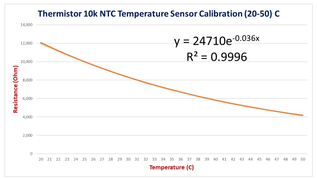
And from this graph we can find this relation:

Where we can get the value of ‘A’ or the analog reading from the sensor output. Note that this formula will only hold when the external resistance used is 10k . If this value is changed, some values in the equation will change as well.
Selection of the Communication Protocol
We have selected Bluetooth Low Energy (BLE), which served us perfectly, as it meets many of our constraints. And it has the following features:
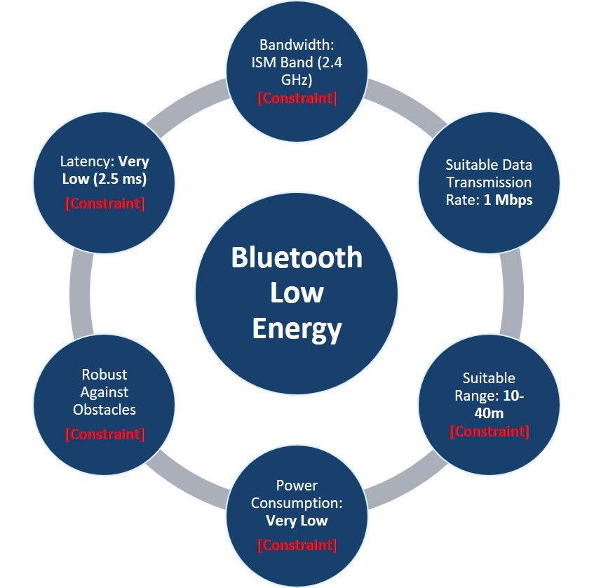
- Very low latency
- ISM Band (2.4GHz)
- Can have a transmission data rate of 1 Mbps
- A good range from 10-40m
- It consumes very low power
- Robust against obstacles
Selection of the Microcontroller Unit (MCU)
The selection of the Microcontroller Unit (MCU) was a tedious task since there are many MCU modules available in the market which can work equally efficiently in making BLE communications. Some of the candidates were esp32 from Espressif, Adafruit Huzzah/Feather, MCUs from nRF semiconductor, Arduino Nano BLE/BLE Sense, etc. Among all these options, esp32 was chosen for the following reasons,
- It comes in small packages
- It has an active online community
- Supports Bluetooth v4.2
- And the most important feature, its low in cost.

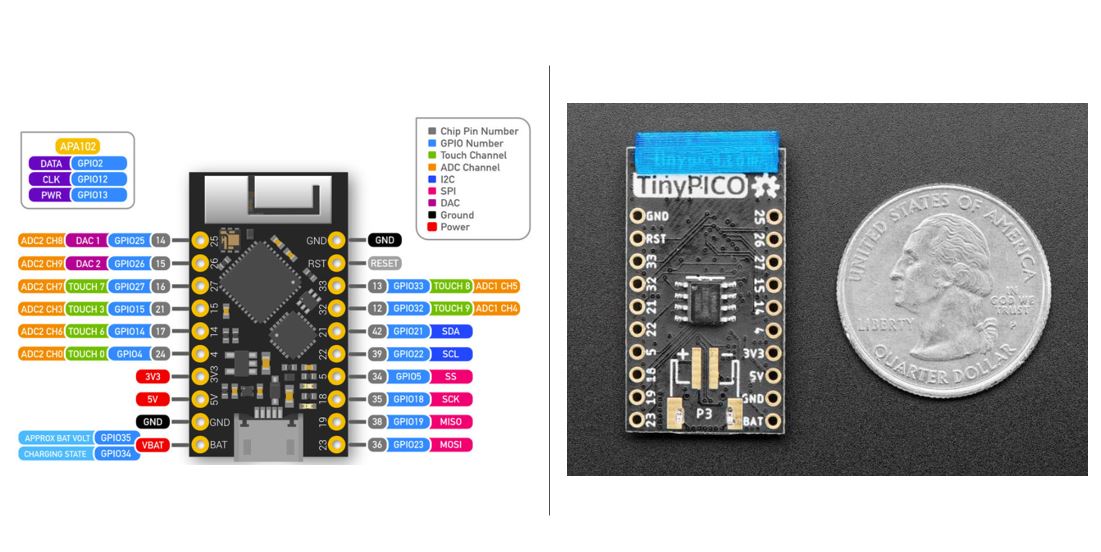
For these reasons, a microcontroller called TinyPICO esp32 module was selected, which satisfies our selection criteria. It has the features that we are looking for, which are:
- First, it has a very small size, and as you can see in the figure below its barely bigger than a coin
- It has enough general input/output pins
- It consumes low power and has a cheap cost
- It can be coded easily
- Its breadboard friendly, which is very important for our case, as it can be connected easily to the breadboard to be tested before its fixed on the printed circuit board (PCB)
- It has constant voltage output using embedded LDO. And finally, it can charge a batter if needed, which is great as well
Coding for the BLE Communication
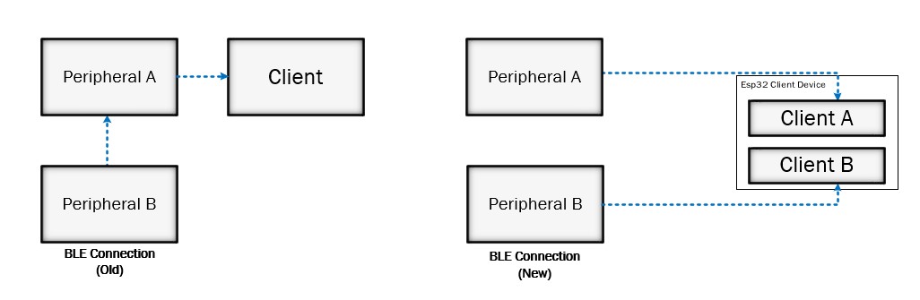
As it can be noticed, in the previous SDP, data was used to go from Peripheral B to Peripheral A and then to the client, so if Peripheral A is not working for some reason then the whole transmission is down.
But for our case we have made each peripheral to transmit the data independently to the central device (Client A and B) to have a robust transmission while transmitting a large packet size.
The code was firstly done in Arduino IDE, then we switched to PlatformIO IDE because of its better debugging capacity, better terminals, better visuals and most importantly, to manage the codes as a project.
Now we have all libraries in that project, which we modified. If we want to share the code to someone, maybe a hospital, we can just send everything in a single folder.
On the contrary in Arduino IDE, libraries should be downloaded and installed, then they should be modified, otherwise the code will not run. This might be very much time consuming for non-experts.
Selection of the Power Supply Unit
The data acquisition device is planned to be portable and rechargeable. It will also be used for human usages, so it must have some sort of protection circuitry embedded. Therefore, the Power Supply Unit should roughly possess the following qualities:
- Light: It should not be heavy enough to impede the Gait Cycle of the subject. Since the PCB is already light and small, using a light power supply unit, which could be a battery, will save the day.
- Small Size: The size of the battery should not exceed the size of the PCB so much. Otherwise, the surface efficiency achieved by reducing the PCB size will go in vain. Lightness and small size will make the hardware much more portable, and suitable for the subjects.
- Ample Charge Storage: The device is planned to be portable. If the charge of the battery perishes very fast, the overall aim of portability will not be justified. So, a power supply unit with a small size but dense enough to store a good amount of energy should be used.
- Safe: The device will be used on a human body, so the safety factor must be assessed. A protection circuitry must be present along with the PCB in order to protect the device from overcurrent, overvoltage, so on and so forth.
- Compatible and Easily Detachable: The battery should be compatible with the hardware specifications and easily detachable for charging.
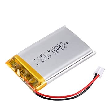
After assessing these basic requirements for the power supply units, the Lithium Polymer (Li-Po) batteries with embedded protection circuitry, as shown in the Figure Below, has been chosen for the project. This battery has other additional benefits such as, the ability to supply high current (can deal with current peaks from BLE Tx/Rx), low self-discharge or charge leaking, possesses a high charge efficiency which allows the battery to be recharge and discharge for a long period of time without being dull (this is mainly due to the chemical efficiency of Li-Po). All these qualities increase the longevity of Li-Po and require low maintenance for the battery.
The chosen Li-Po battery along with its embedded protection circuitry and a built in JST connector is shown below:
Designing the Smart Insole
Stage 1:
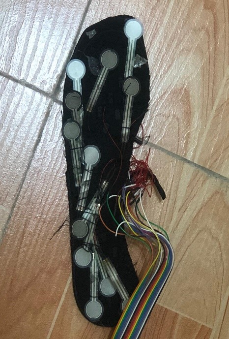
The smart insole designed was based on an attempt by one previous SDP Group. Work was done on it step by step in order to make it compatible with other hardware. Previously, the FSR locations were not optimized compared to the pressure points of the feet. Some of the FSRs were partly outside the insole area, which might affect the readings. Moreover, too many FSRs were crowded in regions where fewer were enough, and some other important areas were kept blank.
Before inserting the FSRs into the insole, critical points around the feet were checked based on similar researches and fitting with a person’s feet. This will help the readings to be more accurate afterward while performing classifications.
The connectors between the smart insole and the PCB was not well made previously, so it had to be redone. In fact, the PCB design is deeply connected to the insole design and the connector used between the insole and the PCB. For this reason, the PCB must be designed two times.
After the insoles were ready, the FSRs were soldered to the ribbon cable, which has 17 pins in one row. Sixteen of those pins were for 16 sensors, and 1 was a common ground.
Stage 2:
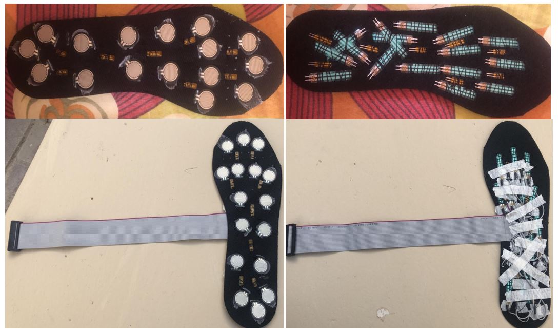
The insoles had to be redesigned after it was decided to include flexible temperature sensors to the insoles. Eight flexible temperature sensors were embedded into each insole, alongside the sixteen FSRs.
The previous ribbon cable used had half of its pins unutilized (i.e., it had 34 pins along two lines, only one line was used). It made the design inefficient as we were using only half of the available resources.
Moreover, the stranded wires from the unused pins were accumulating and causing a bump under the insole. After adding the temperature sensors, the total number of sensors per insole was 24, and one pin is needed for the ground (or the VCC, depends on the PCB design).
So, a ribbon cable with 26 pins (13 pins in each row was chosen), and the PCB model (3rd and 4th) was designed to be compatible with it. Then the ribbons had been soldered to the insole after the insole was ready. Maximum efforts were given to the insole backend since many sensor ends are reaching each other and might cause a short circuit or provide with faulty data if not designed carefully. But the expert technicians at Qatar University were able to solder the ribbon cable to the FSR without any issue. Care was also given while assigning a ribbon cable to a certain sensor. It was important to notice the correct sequence. Otherwise, it will affect a lot in future steps.
The following two figures illustrate the difference between the old insole design model and the new one.
Old Design:
New Design showing all sides:
PCB Design
Patients’ satisfaction, patients’ comfort, and avoidance of electrical hazards are factors of great importance, as the final product is expected to be a wearable system used for medical purposes, or at least a prototype (since commercialization requires much more rigorous treatment). The past model that has been implemented in the previous SDP contained some issues in patients’ comfort while wearing the foot-sole due to the huge size, weight, and thickness of the PCB. For this reason, minimizing and improving the PCB had been a significant goal achieved in this project by identifying the efficient and possible ways of improvement.
So, after going through many design attempts for better improvements. The following figure shows the a comparison between the old PCB Vs. the new PCB:
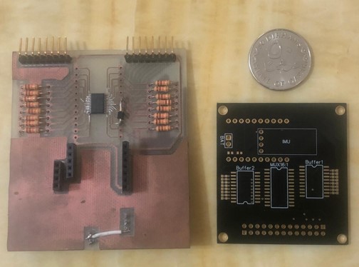
New improvements achieved in the new model are as follows:
- The issue regarding the control pins arrangement for the MUX from TinyPICO was solved
- The Top Silk of the PCB was rewritten in a tidy manner
- Buffers were added to the design for the first time (which slightly increased the PCB size
- Locations of IMU, Battery Pins and other components were rearranged to be in a suitable location
And as we can notice the new PCB has improved significantly, by using SMD components which are very small and the proper use of top and bottom layers. As a result, the area has decreased dramatically by 48% approximately, compared to the older one. Height and weight have decreased as well. Eventually, smaller PCB with smaller height and weight, will afford more comfort to the patient, as its mounted on the leg.
Moreover, the new PCB does not have only a smaller area only but more options as well, which is a good accomplishment we believe.
The old model had the following options:
- Wireless Communication BLE 4.0
- Acquire vGRF – 16 Points
And the options of the new model are as follows:
- Wireless Communication BLE 4.2
- Acquire vGRF – 16 Points
- Acquire Temperature – 8 Points
- Buffers to remove Loading Effect
- Power is managed better, and we can charge our battery
- Inertial Measurement Unit (IMU)
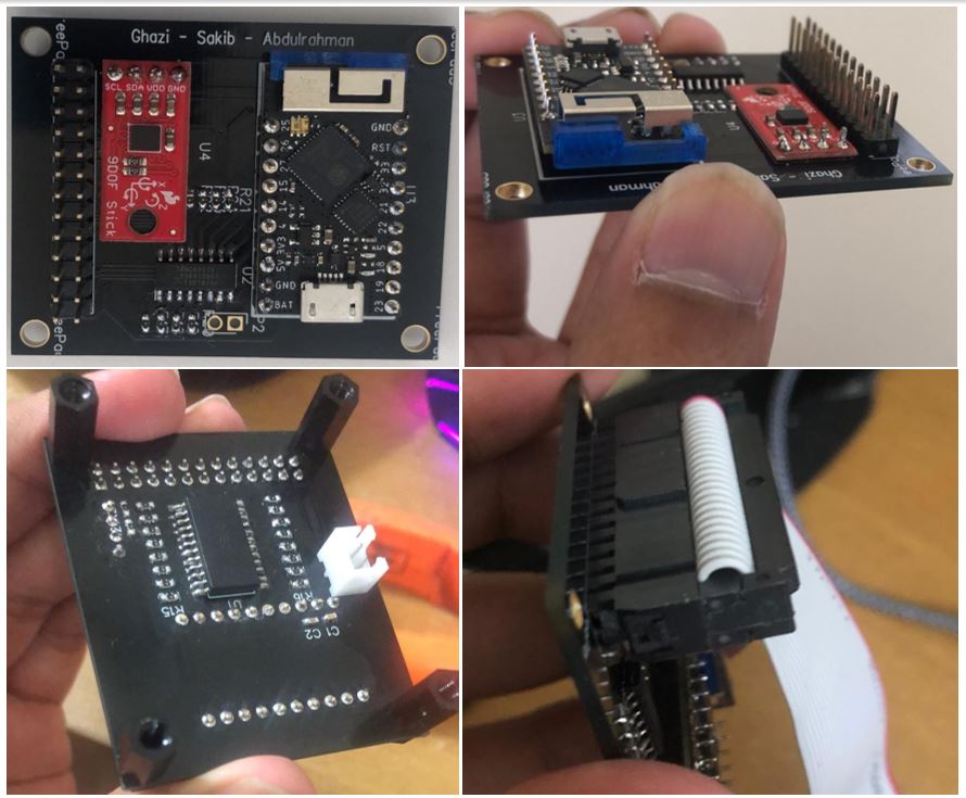
The following picture shows the new PCB with all components soldered on it from all sides, and how the ribbon cable fits perfectly on the PCB:
Unfortunately, at the time we had this PCB ready for execution, our classes were suspended due to CORONA virus (Covid-19) and we could not reach Qatar University labs in order to run the PCB and test it.
Designing a 3D Box for Containing the Hardware
A 3D Box was designed in Fusion360 to keep the PCB along with all its components and circuitry inside. It should be remembered that the device will be worn by a lot of different subjects from different backgrounds, and their idea about electrical circuitry might be multifarious, which might give rise to skepticism about our approach. So, the 3D box was designed, keeping in mind subtle issues like “Patient Perspective about the Device” and overall Aesthetics of the device.
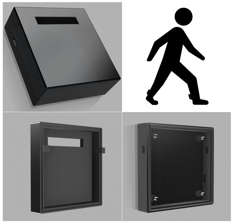
Notable Features:
- Compact and Slick Looking
- Can Screw the PCB tightly
- No Sharp Edges
- Window on top for Ribbon Cables
- Hole in the side for MicroUSB Cable connecting the PCB for Code Uploading or Charging
- Tested thoroughly for debugging 3D Printing Related Issues